Embedded Die Packaging in IC Package Substrate Market Size (2023 – 2030)
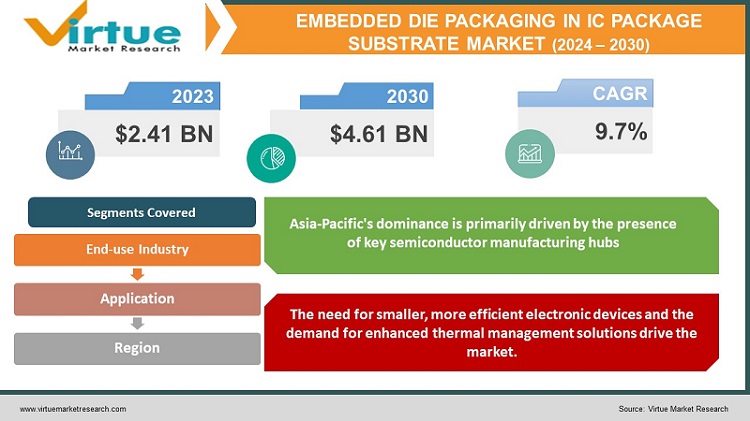
According to the report published by Virtue Market Research in Global Embedded Die Packaging in IC Package Substrate Market was valued at USD 2.41 billion and is projected to reach a market size of USD 4.61 billion by the end of 2030. Over the forecast period of 2024-2030, the market is projected to grow at a CAGR of 9.7%.
Embedded Die Packaging represents a transformative technology within the semiconductor and electronics manufacturing sector. Its core objective is to enhance the performance and efficiency of integrated circuits (ICs) by integrating them directly into substrates. This innovation comes with a distinct array of trends, challenges, and potential advantages that are unique to the semiconductor industry. As the market's appetite for smaller, yet more potent electronic devices continues to soar, the role of Embedded Die Packaging is poised to become increasingly pivotal. Professionals and industry leaders in the semiconductor and electronics sector must remain vigilant in tracking the latest developments and evolving trends within this domain to harness the immense opportunities it offers for both innovation and market expansion.
Key Market Insights:
Embedded Die Packaging in the IC Package Substrate Market presents several key market insights that are shaping the industry's trajectory. First and foremost, there is a growing demand for miniaturization and increased performance in electronic devices, driving the adoption of Embedded Die Packaging as a means to achieve these goals. Furthermore, this technology offers improved thermal management and power efficiency, catering to the evolving needs of various applications, from consumer electronics to automotive systems. Cost-effectiveness is also a significant driver, as the integration of ICs into substrates can lead to reduced production costs. However, challenges such as design complexity and the need for specialized manufacturing processes must be navigated. Overall, the Embedded Die Packaging market is characterized by a delicate balance between innovation, cost considerations, and performance enhancements, making it crucial for industry stakeholders to stay abreast of these trends and insights to remain competitive in this dynamic landscape.
Embedded Die Packaging in IC Package Substrate Market Drivers:
The need for smaller, more efficient electronic devices and the demand for enhanced thermal management solutions drive the market.
The Embedded Die Packaging in the IC Package Substrate Market is being propelled by several compelling drivers. Firstly, the relentless consumer demand for smaller, more powerful, and energy-efficient electronic devices is a primary catalyst. Embedded Die Packaging allows for the miniaturization of integrated circuits, making it ideal for applications like smartphones, wearables, and IoT devices. Additionally, this technology offers improved thermal performance, a critical factor as electronic components become more densely packed and generate higher heat loads. Cost reduction is another significant driver, as it streamlines manufacturing processes and lowers production expenses. Furthermore, the automotive industry's growing reliance on embedded die solutions for advanced driver assistance systems (ADAS) and electric vehicles is fueling market growth. In essence, the Embedded Die Packaging market is driven by a convergence of consumer demand, technological advancements, and cost-effective solutions across a broad spectrum of industries.
The cost reduction and the growing adoption of embedded die technology in automotive applications are significant drivers propelling market growth.
The Embedded Die Packaging in IC Package Substrate Market is witnessing robust growth driven by multiple factors. One pivotal driver is the escalating demand for smaller and more efficient electronic devices. Consumers across the globe seek compact yet powerful gadgets, and embedded die technology plays a critical role in meeting this demand by enabling the miniaturization of integrated circuits. Simultaneously, the industry's heightened focus on thermal management solutions is boosting the adoption of embedded die packaging. As electronic components continue to become more compact and powerful, effective heat dissipation is crucial to maintain optimal performance and longevity. Moreover, cost reduction remains a top priority for manufacturers, and the integration of ICs into substrates streamlines production processes, resulting in cost savings. Lastly, the automotive sector is increasingly relying on embedded die solutions, particularly for advanced driver assistance systems (ADAS) and electric vehicles (EVs). These diverse drivers collectively underscore the growing importance and wide-ranging applications of embedded die packaging in the semiconductor industry.
The increasing government support in research grants and intellectual property protection fosters innovation and provides a conducive environment for growth.
Government support and policies play a vital role in fostering growth and innovation within the Embedded Die Packaging in the IC Package Substrate Market. One of the key ways in which governments assist this industry is through research and development grants and incentives. By offering financial support to companies and research institutions engaged in advancing embedded die technology, governments encourage innovation and the development of cutting-edge solutions. Moreover, regulatory frameworks that promote intellectual property protection help safeguard the investments made by companies in research and development, providing a conducive environment for technology innovation. Additionally, governments can facilitate collaboration between academic institutions and the private sector, creating a synergy that accelerates the pace of technological advancements. Lastly, by promoting initiatives focused on skill development and workforce training in semiconductor and electronics manufacturing, governments can ensure a steady supply of skilled professionals, bolstering the industry's capabilities. Overall, government support in various forms can significantly contribute to the growth and competitiveness of Embedded Die Packaging in the IC Package Substrate Market.

Embedded Die Packaging in IC Package Substrate Market Restraints and Challenges:
Complex design and manufacturing processes, as well as reliability concerns in harsh environments, pose significant challenges.
The Embedded Die Packaging in the IC Package Substrate Market, while promising, is not without its share of restraints and challenges. Firstly, the technology's complexity presents a significant hurdle. The intricate design and manufacturing processes involved can lead to increased development time and costs, which may deter some manufacturers from adopting this approach. Furthermore, ensuring the reliability and long-term performance of embedded die solutions can be challenging, especially in harsh environments or under extreme operating conditions, such as those encountered in automotive or aerospace applications. Supply chain disruptions and material shortages, as witnessed in recent times, can also impact production timelines and increase costs. Additionally, standardization and interoperability issues need to be addressed to facilitate widespread adoption. Lastly, there are concerns regarding intellectual property rights and security in embedded die designs, which can hinder collaboration and innovation. Despite these challenges, the market continues to evolve as advancements are made in addressing these issues, offering promising opportunities for those willing to navigate these complexities.
Embedded Die Packaging in IC Package Substrate Market Opportunities:
The Embedded Die Packaging in the IC Package Substrate Market presents a host of compelling opportunities. Firstly, the growing demand for high-performance and miniaturized electronic devices across various industries, including consumer electronics, automotive, and healthcare, is a substantial opportunity. Embedded die technology's ability to meet these demands positions it favorably for widespread adoption. Moreover, as the semiconductor industry strives for energy efficiency, embedded die packaging offers superior thermal management, which is critical for advanced processors and power-hungry applications. The market also benefits from the increasing emphasis on sustainable and eco-friendly manufacturing processes, as embedded die technology can contribute to reducing material waste and energy consumption. Furthermore, the ongoing research and development efforts to enhance the reliability and longevity of embedded die solutions create opportunities for innovation and market growth. Lastly, as emerging technologies like 5G and the Internet of Things (IoT) gain traction, embedded die packaging is poised to play a pivotal role in enabling the next generation of connected devices. These factors collectively highlight the vast opportunities within Embedded Die Packaging in the IC Package Substrate Market.
EMBEDDED DIE PACKAGING IN IC PACKAGE SUBSTRATE MARKET REPORT COVERAGE:
|
REPORT METRIC
|
DETAILS
|
|
Market Size Available
|
2023 - 2030
|
|
Base Year
|
2023
|
|
Forecast Period
|
2024 - 2030
|
|
CAGR
|
9.7% |
|
Segments Covered
|
By Application, End-use Industry, and Region
|
|
Various Analyses Covered
|
Global, Regional & Country Level Analysis, Segment-Level Analysis, DROC, PESTLE Analysis, Porter’s Five Forces Analysis, Competitive Landscape, Analyst Overview on Investment Opportunities
|
|
Regional Scope
|
North America, Europe, APAC, Latin America, Middle East & Africa
|
|
Key Companies Profiled
|
ASE Group, AT&S, Fujitsu Limited, General Electric, Infineon Technologies AG, Microsemi Corporation, STMicroelectronics, TDK Corporation, Texas Instruments Incorporation, Toshiba Corporation
|
Embedded Die Packaging in IC Package Substrate Market Segmentation: By Application
-
Smartphone & Tablets
-
Medical Implants and Wearable Devices
-
Industrial Sensing Devices
-
Industrial Controlling Devices
-
Industrial Metering Devices
-
Military Communication & Power Devices
-
Others
In the Embedded Die Packaging in IC Package Substrate Market, the largest market share belongs is held by the Smartphone and tablets segment, primarily due to the incessant demand for compact yet high-performance electronic components in the smartphone and tablet industry. These devices heavily rely on embedded die packaging to achieve their sleek and efficient designs, propelling this segment to the forefront of the market. While the Medical Implants and Wearable Devices segment exhibits the fastest growth rate. The healthcare sector increasingly integrates advanced electronics into medical implants and wearable health devices for remote monitoring and diagnostics, driving the demand for embedded die packaging as the industry seeks compact and efficient electronic solutions. This trend is expected to persist as the medical field continues to embrace sophisticated electronics for enhanced patient care and monitoring.
Embedded Die Packaging in IC Package Substrate Market Segmentation: By End-use Industry
-
Consumer Electronics
-
IT & Telecommunication
-
Healthcare
-
Aerospace & Defense
-
Automotive
-
Others
In the Embedded Die Packaging in IC Package Substrate Market, the segment with the largest market share is the Consumer Electronics industry. This dominance can be attributed to the ever-increasing demand for smaller, more powerful, and energy-efficient electronic devices such as smartphones, wearables, and laptops. Consumer Electronics continually pushes the boundaries of technology, driving the adoption of embedded die packaging to achieve miniaturization and enhanced performance. On the other hand, the segment with the fastest growth is the Healthcare industry. The healthcare sector's rapid adoption of embedded die technology is primarily driven by the need for compact, high-performance medical devices and equipment. These advancements in embedded die packaging offer improved functionality, smaller form factors, and enhanced data processing capabilities, making it an essential component in the evolving landscape of healthcare technology.

Embedded Die Packaging in IC Package Substrate Market Segmentation: Regional Analysis
-
North America
-
Asia-Pacific
-
Europe
-
South America
-
Middle East and Africa
In the Embedded Die Packaging in the IC Package Substrate Market, currently, the largest market share can be attributed to the Asia-Pacific region. Asia-Pacific's dominance is primarily driven by the presence of key semiconductor manufacturing hubs, including Taiwan, South Korea, and China. These countries are at the forefront of semiconductor production, contributing significantly to the adoption of embedded die packaging due to their expertise in electronics manufacturing. Additionally, the region's robust consumer electronics market and the growing demand for advanced automotive technologies further bolster its market share. On the other hand, the Middle East and Africa are poised for the fastest growth in this market. While currently a smaller segment, this region is experiencing a surge in infrastructure development, digitization initiatives, and an expanding electronics industry. As a result, there's an increasing demand for embedded die packaging technology to support these developments, making it a promising growth area.
COVID-19 Impact Analysis on the Global Embedded Die Packaging in IC Package Substrate Market:
The COVID-19 pandemic had a notable impact on the Embedded Die Packaging in IC Package Substrate Market. Like many industries, this market faced several challenges during the pandemic. Supply chain disruptions, caused by factory shutdowns and transportation restrictions, led to delays in manufacturing and delivery of essential components, affecting production schedules and increasing costs. Moreover, travel restrictions and lockdowns hindered the collaboration and coordination necessary for research and development efforts, potentially slowing down innovation. However, on the flip side, the pandemic accelerated the adoption of remote working and telemedicine, increasing the demand for high-performance electronic devices and healthcare equipment, which in turn boosted the Embedded Die Packaging market in these specific segments. The overall impact was a mix of challenges and opportunities, with the long-term effects emphasizing the importance of resilient supply chains and adaptable business strategies in the semiconductor and electronics industry.
Latest Trends/ Developments:
The Embedded Die Packaging in IC Package Substrate Market serves as a critical enabler for various other industries. Its innovative technology, which enhances the performance and efficiency of integrated circuits by embedding them within substrates, has far-reaching implications. In the Consumer Electronics sector, it facilitates the development of smaller and more powerful devices, driving the market for smartphones, tablets, and wearables. In the Automotive industry, embedded die packaging supports advanced driver assistance systems (ADAS) and electric vehicle (EV) technologies, contributing to safer and more efficient transportation. Healthcare benefits from embedded die solutions by enabling compact and high-performance medical devices, improving patient care and diagnostics. Moreover, the Aerospace and Defense sector relies on this technology for ruggedized and miniaturized electronics used in critical applications. In essence, Embedded Die Packaging acts as a technological catalyst that empowers various markets to innovate, optimize, and advance their offerings, thereby fostering progress across multiple industries.
Key Players:
-
ASE Group
-
AT&S
-
Fujitsu Limited
-
General Electric
-
Infineon Technologies AG
-
Microsemi Corporation
-
STMicroelectronics
-
TDK Corporation
-
Texas Instruments Incorporation
-
Toshiba Corporation


