“Advanced packaging is no longer the final step of manufacturing; it is now a core part of chip design strategy.”
The advanced packaging is becoming as important as wafer fabrication nowadays by replacing wafer fabrication as only critical part of semiconductor industry. Main limitation is no longer the shrinking of transistors, but rather the industry’s ability to package complex chips, secure specialized materials, and obtain sufficient high-performance memory to support next-generation computing workloads. Advanced packaging demands specialized infrastructure, materials, and logistics to integrates multiple chips, memory modules, and substrates into a single system. Shortages in substrates, cold chain handling, and HBM production now show up first in AI chips and GPUs, reshaping the global supply chain and redefining competitive advantage.
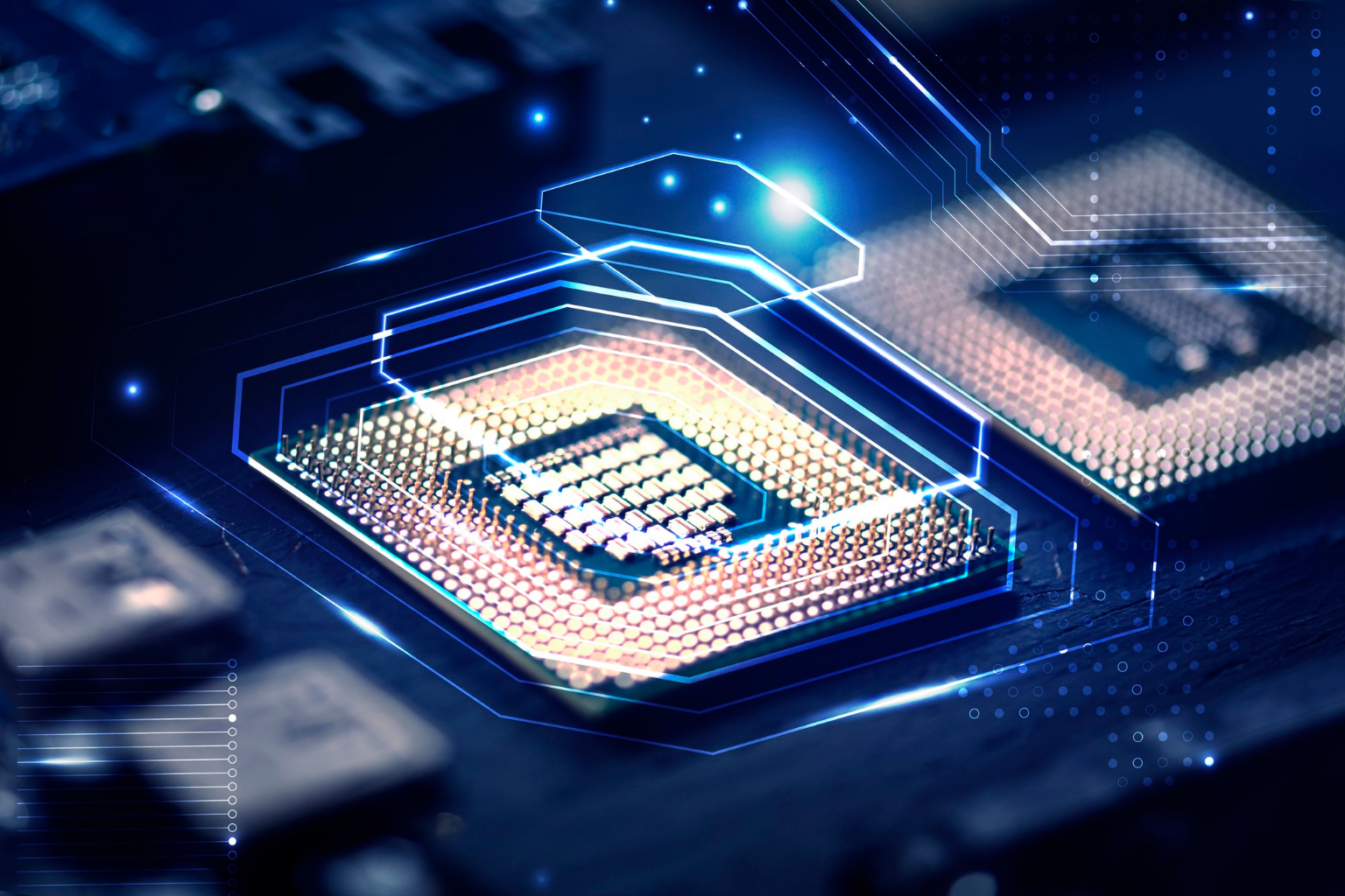
Advanced Packaging Is the New Fab: Why Advanced Packaging Now Matters More Than Ever?
The progress of semiconductor used to define by Moore’s Law of shrinking transistors to deliver faster, cheaper, and more efficient chips. However now advanced packaging has emerged as the new frontier by enabling heterogeneous integration, chaplet architectures, and high‑bandwidth memory (HBM) solutions that power AI accelerators and high‑performance computing. Thus, the semiconductor industry is shifting to system level scaling from traditional transistor scaling.
Why Industry Response is shifting from Transistor Scaling to System Level Scaling?
- Transistor Scaling: Due to quantum thermal limitation, the shrinking of transistors as per Moore’s principle is no longer delivering exponential gains in semiconductor industry.
- System Integration: Advanced packaging gives more effective performance by extending innovation beyond transistor miniaturization by integrating chip into a system on package, optimizing interconnects, and reducing latency.
What is Moore’s Law?
According to co‑founder of Intel Gordon Moore’s principle, the number of transistors on a microchip roughly doubles every two years, leading to exponential growth in computing power while reducing cost per transistor. Moore’s principle is facing limitation due to leakage in gates, heat and reliability challenges with economical limits such as the costs of next‑gen fabs and lithography tools, due to which scaling becoming unsustainable. Technological advancements further changing the industry response for this principle. Companies are investing in advance packaging technologies like 2.5D/3D stacking, hybrid bonding, and co‑packaged optics.
Rise of Chiplets, AI Accelerators, and HPC Workloads:
- Chiplet Architectures: Architectures for chiplets design allows flexible scaling and faster innovation by breaking monolithic designs into modular chiplets.
- AI Accelerators: GPUs and AI chips rely on advanced packaging to integrate HBM and deliver massive bandwidth. So, growing adoption of AI and demand of advance computer driving demand for advance packaging
- HPC Workloads: Data centers, scientific computing, and edge AI demand packaging solutions that balance speed, efficiency, and power.
Advanced packaging has become new engine of semiconductor progress and no longer just a backend process. The industry can overcome Moore’s Law limits and meet the demands of AI, HPC, and next‑generation workloads by shifting from transistor scaling to system level scaling. The shortages in substrates, HBM, and packaging capacity increasingly dictate who leads and who lags, thus companies with master in advanced packaging will define the future of computing.
From Fab Bottlenecks to Packaging Bottlenecks: Why Wafer Capacity Is No Longer the First Constraint?
Traditionally, bottlenecks of semiconductor industry were measured in lithography nodes and fab throughput, because the progress of semiconductor industry was defined by wafer fabrication capacity. Now the new limiting factor of semiconductor industry have shifted to assembly, testing, substrates, and integration, because the progress of semiconductor industry is defined by advance packaging. This transition of fab bottlenecks to packaging bottlenecks reflects the slowdown of Moore’s Law. The demand for advance sophisticated packaging solutions is further driven by rise of artificial intelligence, HPC, and chiplet based architectures.
Why Wafer Capacity Is No Longer the First Constraint?
The wafer capacity is no longer the first constraint, because wafer output has increased due to installation of new fabrication plants globally, still there is mismatches between wafer supply and packaged chip availability because the back-end processes of semiconductor manufacturing have not scaled at the same pace. Due to limitation in packaging capacity, sometimes fabricated chips sit idle for further procedure. Thus, actual bottlenecks in semiconductor industry are shifting, wafer capacity is no longer the first constraint advance packaging capacity is new bottlenecks.
How Back-End Operations Now Determine Shipping Schedules
- Assembly and testing delays: It is very crucial to reduce production cycle. HBM integration and complex packaging steps, such as 2.5D/3D stacking, hybrid bonding takes longer than conventional assembly.
- Substrate scarcity: A small number of suppliers for advanced substrates can hold up deliveries even when wafers are finished.
- Cold-chain and special handling: Certain chips (for example, AI accelerators with HBM) may require biologics-like logistics, adding transport and handling complexity.
What "Advanced Packaging" is actually includes:
Advanced packaging is the new frontier of innovation in the field of semiconductors. In the wake of slowing down of Moore's law, the performance improvements are now being achieved by the integration of multiple dies or chiplets, or memory pillars in what are now termed as "advanced packages" which facilitate more innovations in 2.5d/3d packaging, heterogeneous integration, and advanced interconnect solutions by using advanced substrates and interposers.

- 2.5D Packaging: Advanced 2.5D packaging is characterized by the use of an interposer layer (silicon or organic) for connection of more than one die side by side. This ensures significantly increased bandwidths and reduced latencies than traditional PCB solution for communication.
- 3D Packaging: Active circuitry or dies are stacked vertically across each other and connected either through "through-silicon vias" (TSVs). This significantly reduces the die footprint and the distance followed by interconnects.
In both advanced 2.5D packaging and 3D packaging approaches, logic, memory and specialized accelerators are integrated to obtain compact, high-performing systems.
Chiplets and Heterogeneous Integration:
- Chiplets: Small modular dies assembled to form a system on package. Systems comprising chiplets have more flexibility, faster design cycles, and cost effective.
- Heterogeneous Integration: Assembling multiple types of chips (CPU, GPU, AI accelerators, memory) in one package to optimize workload handling dynamically.
Role of Advanced Interconnects and Substrates:
- Interconnects: High bandwidth, low latency connection technologies, such as hybrid bonding and advanced interposers, will facilitate chiplet communication.
- Substrates: Special materials will support the mechanical and electrical needs of various new systems. The power delivery, electrical, electronic, and thermal performance driving demands for advance substrates.
Advanced packaging is the new engine of semiconductor progress and not just backend process. By enabling 2.5D/3D integration, chiplet architectures, and advanced interconnects, packaging defines how modern chips achieve performance, efficiency, and scalability. As the industry shifts from transistor scaling to system level scaling, advanced packaging determines who leads in AI, HPC, and next‑generation computing.
The discovery of Substrate Supply as the Constriction in High-tech Semiconductor Packaging.
One of the weakest links in the semiconductor chain is substrate supply that is characterized by limited capacity of suppliers, geographic concentration and slow growth cycles. Ajinomoto Build-Up Film (ABF) substrate is a critical, high-performance insulation material developed by Ajinomoto for semiconductor packaging, enabling fine-circuitry (2/2 µm) and high-density interconnections for CPUs, GPUs, and AI processors.
Significance of ABF Substrates to Advanced Packages.
- Electrical Role: The ABF substrates are used to provide insulation, routing of signals, and delivery of power between chips and printed circuit boards.
- Performance Enabler: They are essential to high-bandwidth memory (HBM), chiplet integration, and 2.5D/3D packaging.
- Industry Reliance: Virtually every sophisticated processor in GPUs to AI accelerator is dependent on ABF substrates to deliver a high-performance platform.
Why Substrate Capacity Lags Chip Demand?
- Complexity of Manufacturing: The production of ABF substrates involves specialized chemistry and multiple layering which makes it difficult to scale up.
- Slow Ramp-Up: The construction of new substrate facilities requires years as compared to quicker fab expansions.
- Demand Surge: AI workloads and HPC systems use a much higher count of substrates per package, surpassing the increase in supply.
Supplier Concentration in Geographic Terms.
- Regional Dependence: Almost all ABF substrate production is focused in Japan, Taiwan and some other areas.
- Supply Chain Risk: Geographic conglomeration results in exposure to geopolitical strains, natural catastrophes, or export taxes.
- Low Diversification: There are not a large number of new entrants and the global chipmakers rely on a few suppliers.
Supplies of substrates have turned out to be an understated bottleneck in advanced packaging. ABF substrates have become a necessity in current chip designs but capacity lags behind the need because of the complex manufacturing and geographic concentration. Substrate availability will become the determining factor in the delivery times, with the increasing AI loads and HPC loads. It will be necessary to invest in new substrate plants, diversify suppliers and work more closely between chipmakers and materials companies, to deal with this bottleneck.
Dependency of High Bandwidth Memory (HBM) on the Complex Packaging Procedures
High Bandwidth Memory (HBM) is becoming essential for AI accelerator chips and high-performance computing (HPC) machines. Traditional DRAM Stacks memory dies horizontally and connects to peripheral components through advanced packaging solutions, such as HBM on the other hand offers enormous potential bandwidth by stacking memory vertically. Yet, this reliance on packaging brings complexity and capacity limitations and supply risks throughout the semiconductor supply chain.
Why HBM Is So Important for AI and HPC Chips
- Bandwidth Requirements: AI training and workloads inference necessitate fast data movement between the processors and memory which is driving demand of high bandwidth memory (HBM).
- Energy Efficient: HBM reduces energy consumption in comparison to traditional memory architectures to address different needs of energy in HPC systems.
- Scaling in Performance: HBM is the foundational technology for achieving terabytes per second of bandwidth in GPUs, TPUs and AI accelerators.
Packaging Complexity for Stack and Integration:
- 3D Stacking: HBM involves using through‑silicon vias (TSVs) to establish vertical connections between multiple memory dies.
- Integration with Logic: Advanced packaging integrates HBM with CPUs, GPUs or AI accelerators on either interposers or substrates.
- Thermal difficulties: Stacking adds thermal density (heat), which is why advance packaging and sophisticated cooling designs are required.
Why HBM Shortages Lead to Delays at The System Level?
- Supply Bottlenecks: Advance packaging is the bottleneck on chip shipments, even after wafers are ready, due to fewer and smaller HBM suppliers,
- Impact for the System: AI server, HPC clusters and data center are executed a delay at the system level because of outdated HBM module.
- Industry Ripple: HBM packaging shortages are impacting entire ecosystems from cloud providers to consumer GPUs.
HBM’s bandwidth and efficiency potential is accompanied by a reliance on advanced packaging. AI and HPC chips do not operate at scale without proven, high-bandwidth memory integrated, yet packaging complexity and supply availability tend to determine when shipments occur. The solutions to address HBM packaging bottlenecks will be important in enabling the continuation of advancement in next‑generation computing, with the increasing demand for generative AI and scientific computing.
Packaging as Next Control Point in Semiconductor Supply Chains and Chip Shipments
Traditionally, semiconductor advancement was described by wafer manufacturing capacity. However advanced packaging is the new control point in the supply chain. Shipment timing, demand signals and industry choke on us are now defined less by the fab itself and more at the back end where substrates, interposers and high‑bandwidth memory (HBM) integration occur.
Why Shipment Timing Is Now Decided at the Back End?
- Fab Output vs Packaging Capacity: Semiconductor fabs can produce large scale wafer but the process of chips manufacturing is incomplete until it is packaged.
- Complicated Processes: Chiplet Integration, 2.5D/3D Stacking & HBM assembly are complicated procedure, which further delays supply chain.
How Ignoring Packaging Creates False Demand Signals?
- Overestimated Fab Demand: Many companies consider wafer output capacity as market supply, which is not accurate but analyzing packaging shows real market demand.
- Bottlenecks in the Supply Chain: Ignoring packaging constraints leads to misaligned forecasts and inventory imbalances. Limitation in packaging leads to supply backlog, which creates unnatural spikes of demand, even when the industry is in downstream.
- Market Distortion: Ignoring packaging constraints leads to misaligned forecasts and inventory imbalances.
Packaging Capacity as the New Industry Choke Point:
- Substrate Shortfall: ABF substrates are not only limited but also geographically concentrated and prone to disruption, causing bottlenecks in advance packaging and overall supply chain.
- HBM Integration: The packaging complexity forces the HBM to rely on the TSV stack and interposer assembly, which is further causing bottlenecks in advance packaging and overall supply chain.
- Industry Impact: AI accelerators, HPC systems, and GPUs face delays even when fabs are fully utilized.
Identifying Where Shortages Appear First in the Semiconductor Supply Chain
Semiconductor supply chains are depending on both wafer fabrication and advance packaging capacity. Packaging backlogs, delays between wafer completion and shipment, and early warning signals in assembly and testing now dictate timelines.

Packaging Backlog vs Fab Utilization
- Fab Expansion: Fabs around the world are operating at full capacity creating wafers in record quantity. Both fab installation and fab’s wafer capacity are expanding.
- Packaging bottleneck: Although the wafer capacity is expanding but the back-end capacity is not expanded at the same speed; it formed mismatches between wafer supply and chip packaging demand.
Interval Of Time Between Wafer Completion and Final Shipment
- Incomplete Inventory: Growing waiting time of wafers at storage for packaging extending supply chain.
- Lengthy Processes: Advanced packaging steps including 2.5D/3D stacking, HBM integration and substrate assembly require more time than conventional assembly.
Early Warning Signals in Back‑End Operations
- Increasing Lead Times: Extending waits for substrates and interposers suggest components of the package process are beginning to form a bottleneck.
- Queue Build‑Up: Increasing backlog in assembly and test houses are a sign of systemic stress.
- Supplier Concentration: Geographic clustering of substrate and packaging suppliers magnifies risks of disruption.
Thus, Shortages in the semiconductor supply chain now appear first in packaging and back‑end operations, not fabs. Resolving these bottlenecks will entail investment in packaging capacity, diversification of substrate suppliers, and greater synchronization of fabs with back‑end partners.
|
|
Fabs (Wafer Fabrication) |
Advanced Packaging (Capacity, Substrates, HBM) |
|
|
Capacity |
Large‑scale global investments; capacity expanded rapidly with Moore’s Law scaling. |
Limited qualified packaging lines; slower expansion cycles; capacity lags behind wafer output. |
|
|
Substrates |
Traditional packaging used simpler substrates; supply was stable and diversified. |
Relies on ABF substrates; supply is geographically concentrated (Japan, Taiwan); shortages often occur first. |
|
|
HBM (High‑Bandwidth Memory) |
Fabs produce memory dies; integration was not historically a bottleneck. |
HBM requires 3D stacking, TSVs, and interposers; packaging complexity makes HBM availability dependent on back‑end processes. |
|
|
Bottleneck Location |
Historically, bottlenecks were in lithography, yield, and fab utilization. |
Today, bottlenecks appear first in packaging: substrate shortages, HBM integration delays, and limited lines. |
|
|
Expansion Cycles |
Capital intensive but supported by global investments; lead times ~2 to 3 years. |
Even slower ramp‑up; requires specialized expertise; often lags demand by several years. |
|
Advanced packaging has emerged as a major bottleneck in the semiconductor industry, causing the limitations to shift from wafer fabrication to back, end processes. The shipment schedules of chips no longer depend most on the utilization of fabs but rather on factors such as capacity constraints, substrate shortages, and the complexity of integrating high, bandwidth memory (HBM). Solving these problems will need investing in packaging capacity, supplier diversification, and carefully planning so that innovation can be converted to product availability in time.
Author:
Amit Mirdha
Associate Research Analyst
https://www.linkedin.com/in/amit-mirdha-577a5a264/
RECENT POSTS

Network Detection & Response (NDR) Market
28 Apr 2026
Liquid Cooling for High-Density Market
28 Apr 2026